填平片上系统设计和制造供应链中的沟通鸿沟
Reading, UK -- May 10, 2022 --As chip supply chains consist of a series of different subcontractors each independently doing a specific task, disconnects can easily happen between them. Sondrel calls these Communication Chasms and warns that they can cause issues that ripple through the rest of the chain adding delays and unexpected costs as stages have to be rescheduled.
Ian Walsh, Sondrel’s VP ASIC Business Development, explained; “Unless the handover between each stage is overseen by someone who really understand the whole process, it is all too easy for there to be a breakdown in communications as assumptions can be made by one or both subcontractors in the chain as to exactly what the status is at handover. In such a Communication Chasm, each will blame the other and the project stalls. With so many stages in a chip supply chain where this could happen many times, the whole project is subject to the risk of serious delays. And, as chips become ever more complex, this risk just increases.
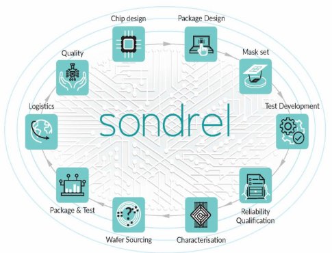
“The overall budget of a new chip project of the type of complex, state-of-the-art SoCs that we specialise in can run into many millions of dollars so customers want to mitigate the risks as much as possible. That is why we offer a complete turnkey service from concept to shipping silicon so that there is no possibility of any Communication Chasms because we take total responsibility for the smooth running of every stage and every subcontractor in the chain. Any issues are spotted and corrective actions taken such as rescheduling tasks or even running some in parallel to keep the project on time which is easy to do when all the stages are being controlled by one company. We have perfected the skills of highly detailed, project management with our own sophisticated, interconnected work flows from all the hundreds of advanced chips that we have designed for customers and we now use these skills for the chip manufacturing chain.”
Sondrel often starts the chip project right at the concept planning stage, where the Power Performance Area (PPA), market requirements and final price point form the foundation for the project. The final price per unit is a key data point as it determines how to produce the chip, i.e., which process and technology node to use and the number of die per wafer that are required to obtain the per die cost. For example, there is no point using latest node to achieve a lower power consumption if the end price cannot support the higher cost of this technology.
Similarly, planning is done for stages further downstream such as the number, size and location of testing pads, the number of pins and what kind of packaging will be required. All too often the Design for Test and Design for Manufacture are not thought of by a pure Design Services company and, as a result, the largest Communication Chasm opens up between the Design company who hands over the GDSII to whoever is doing the actual chip testing and manufacture. For example, with testing, who better to design the test regime for the chip than the engineers who designed it and who better to fix any bugs that testing reveals. Having this the responsibility of one company such as Sondrel with a holistic overview, ensures smooth communication up and down the entire chain, mitigating risk for the customer for on budget and on time delivery.

About Sondrel™
Founded in 2002, Sondrel is the trusted partner of choice for handling every stage of an IC's creation. Its award-winning, define and design ASIC consulting capability is fully complemented by its turnkey services to transform designs into tested, volume-packaged silicon chips. This single point of contact for the entire supply chain process ensures low risk and faster times to market. Headquartered in the UK, Sondrel supports customers around the world via its offices in China, India, Morocco and North America. For more information, visit www.sondrel.com
Related Semiconductor IP
- UCIe D2D Adapter & PHY Integrated IP
- Low Dropout (LDO) Regulator
- 16-Bit xSPI PSRAM PHY
- MIPI CSI-2 CSE2 Security Module
- ASIL B Compliant MIPI CSI-2 CSE2 Security Module
Related News
- ShortLink AB 加入 X-FAB 设计与供应链合作网络及 IP 平台
- 法国Dolphin Design 深化与 GoAsic 的合作关系,加强半导体行业供应链
- Cycuity 与 SiFive、BAE Systems 联手强化微电子设计供应链安全
- Synopsys推进虚拟原型技术可支持系统和半导体供应链合作缔造下一代SoC