Overview
Serial ATA (SATA) is computer bus standard that have the primary function of transferring data between Host and mass storage devices such as HDD and SSD. Serial ATA’s replaced the older Parallel ATA (PATA) standard by offering several advantages such as reduced cable size, hot plugging, faster data transfer through higher signalling rates etc.
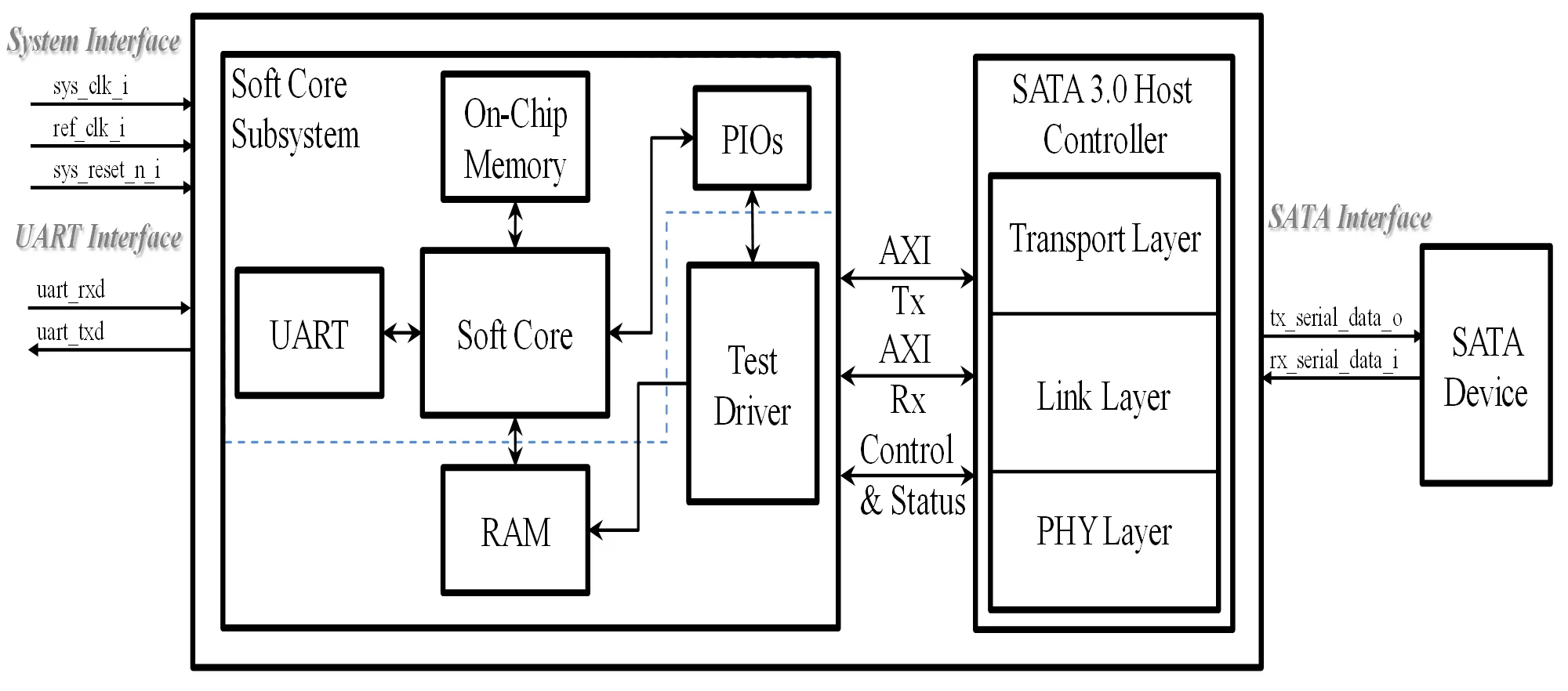
iWaves’s SATA 3.0 Host Controller is available for integration into host FPGA designs to provide an industry- compliant SATA 1.0, SATA 2.0 and SATA 3.0 interface standards. Some of the main features of SATA 3.0 Host Controller are Compliant with the Serial ATA specification revision 3.0, RX Elastic buffer to handle TX and RX frequency variance, 4KB FIFO implemented by Memory block in transmit and receive paths, 32-bit internal data path , Supports AXI Interface to the Application Layer etc.
With iWaves’s SATA 3.0 Host Controller, can gain read/write speed close to maximum read/write of mass storage device. For Transcend SSD , maximum write and read speed are 500MB/s and 560 MB/s respectively. As per performance chart (Figure 2), achieves Write speed of 487MB/s and Read speed of 540MB/s.
iWave’s SATA 3.0 Host Controller consist of 3 layers, Transport Layer, Link Layer and PHY Layer.
PHY Layer: The main functions are converts 32 bit parallel data to differential Tx data and received Rx serial data to 32 bit parallel data, Clock recovery from serial data, 8B/10B encoding and decoding, Byte ordering and word alignment, Speed Negotiation, Out-of-Band (OOB) signal generation and detection.
Link Layer: The link layer is responsible for the transmission and reception of the frames also performs scrambling or de-scrambling and CRC calculations. It also handles flow control and transmission & reception errors.
Transport Layer: The transport layer communicates with the application layer, over the AXI interface, and from the data received formulates the FIS content and while sending back decomposes it. This layer decides the commands supported for the data transfers. It also has buffers in transmit and receive paths to ensure flow control.
IP Validation and Performance Testing:
iWave provides evaluation design can help validate the functionality & performance of the SATA 3.0 Host Controller. Evaluation platform is the Arria 10 SX SoC Development Board with iWave’s FMC Add On-card.
Soft Core Subsystem is used to provide control of the test driver to the user via UART. It performs throughput calculation for write and read, read ID of the SATA device, controls the operation of test driver based on selected test and allows user to Check Write/Read Performance and perform write to and read back from specified address for the defined size. Test Driver module is responsible to generate required signals for performing required operation as requested by user. This module accepts inputs from Soft Core and appropriately the state machine is built to perform the function. Initially the device ID is read and written to the RAM for Soft Core to access. Also the data integrity check in case of read back is done here.
Learn more about SATA Controller IP core
Many times we are not aware of very useful EDA tool options which are already available. Even if such options are very well documented, we don't look at them and try them. But some options are very useful and if you know them, it makes job of design engineer and/or verification engineer very easy. Here, I am going to talk about one very powerful and useful VSIM option of QuestaSim. It is VCDSTIM option of VSIM.
The paper describes the methodology used for functional verification of the USB 3.0 device controller core. The core model has been developed at two different levels of abstraction: RTL model for synthesis and SystemC TLM model for high speed simulation, early software development and early test-bench creation.
Oftentimes, in order to save on the cost of IP, a company will select an encrypted netlist as the deliverable instead of the RTL source code. This is especially common among companies looking to develop in FPGA devices where they can often get the necessary IP from their FPGA vendor.
To support High Definition Television (HDTV) application, the System on Chip (SoC) presented in this paper has to support multiple and concurrent internal processes. Most of these operations read data from memory, process them and store the resulting data into memory. Each functional unit of the system is responsible for a specific data processing, but all the data are stored in the same shared external memories.
Eric Esteve
Eric Esteve