Provider

VeriSyno Microelectronics Co., Ltd.
HQ:
The People's Republic of China
VeriSyno Microelectronics Co., Ltd. is a national high-tech enterprise dedicated to the research and development of semiconductor IPs. The company’s main products include mixed-signal high-speed interface IPs such as USB, HDMI, DDR, MIPI, PCIe, SATA, and various analog IPs such as ADC, DAC, PLL, LVDS, as well as independently developed PSRAM interface IO solutions and vMAC series IPs. As one of the important semiconductor IP suppliers in China, in active collaboration with local foundries, VeriSyno has long been committed to the porting of those mature interface IPs to processes such as 22/28/40/55nm, to ensure secure and reliable supply of domestic IPs. The company’s diversified IP products have been widely used in industries such as industrial, medical, AI, and IoT. VeriSyno was established in September 2018 and is headquartered in Hefei, Anhui, with branch offices in Beijing, Shanghai, and Shenzhen.
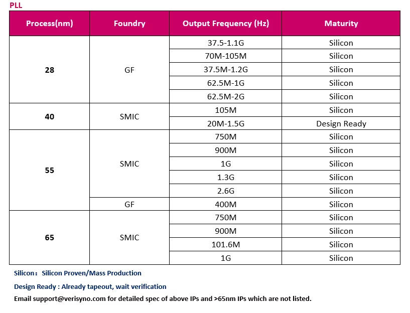
Learn more about PLL IP core
How do you ensure that every part of a system receives the clock it needs—without wasting power or sacrificing performance? The answer lies in creating a well-structured frequency plan built around a PLL.
Jian Yang, Sween Kang (Synopsys)
This white paper is aimed at system architects and physical implementation leaders working on the design of SoCs. It can be confusing to understand the impact of different jitter sources and how to calculate a jitter budget when specifying a digital system. This white paper explains how jitter changes the period of a clock and how to ensure that jitter has correctly been accounted for in the calculations for timing closure.
This article explains a some of the key terminology and parameters commonly used to describe jitter. It will also help clarify the most important parameters for a some PLL applications, allowing the designer to better understand what is required from a PLL.
In high end RF systems, such as 5G radios, the requirements are so stringent that the source of this strongest unwanted tone can be the PLL. This article outlines how spurs in the input clock to the ADC or DAC may limit the SFDR. This in turn will set the requirements for the spurs for the input clock (from a PLL), in order to achieve a specific SFDR.
This article compares analog, first-generation digital, and second-generation digital PLLs. It evaluates which type of PLL may be best in which situation. It further discloses a roadmap into other application areas, including general purpose / logic clocking, and regular low-jitter PLLs.