How Secure DDR Interfaces Protect DRAM from Memory Attacks
Brett Murdock, Dana Neustadter (Synopsys)
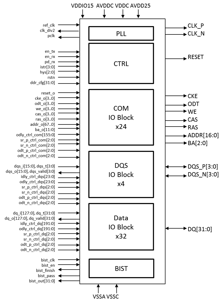
The T40LP_DDR3TOPV01 IP is a high-speed interface for high-performance DDR3 PHY applications.
| Foundry | Node | Process | Maturity |
|---|---|---|---|
| TSMC | 40nm | LP eFlash | Available on request |

high-speed interface for high-performance DDR3 PHY is a DDR IP core from VEGA Semiconductor listed on Semi IP Hub. It is listed with support for tsmc Available on request.
Engineers should review the overview, key features, supported foundries and nodes, maturity, deliverables, and provider information before shortlisting this DDR IP.
Yes. Buyers can compare this product with similar semiconductor IP cores or IP families based on category, provider, process options, and structured technical specifications.