The CMS0069 DVB-CID Modulator provides all the necessary processing steps to modulate the Content-ID table into a complex I/Q signal for input to a pair of DACs, or interpolating DAC devices such as the AD9857/AD9957 or RF DACs such as the AD9789. Optionally the output can be selected as an IF to supply a single DAC.
The design has been optimised to provide excellent performance in low cost FPGA devices such as the Cyclone range from Altera or the Spartan range from Xilinx
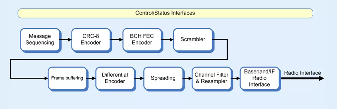
A description of the processing steps follows:
Message Sequencing. The software provided hardware Content-ID table is automatically scanned before being output in the required sequence together with the Unique-Word as required by the DVB-CID specification. Alternatively, a fixed hardware Content-ID table may be used – further reducing the processing overhead required for the DVB-CID modulator core.
CRC-8 Encoding. An 8-bit CRC is added to each Content-ID packet and serves to allow packet-level error detection at the receiver.
BCH Encoding. Each Content-ID packet is protected through a (127, 85) 6-error correcting systematic BCH code before being scrambled.
Scrambling. All the bits within the DVB-CID frame are scrambled for energy dispersal using the DVB randomisation polynomial 1+x5+x9.
Frame buffering and differential encoding. Each DVB-CID frame is buffered and differential encoded prior to implementation of the spreading algorithm.
Spreading. Each DVB-CID is ‘chipped’ to the appropriate rate as determined by the host carrier baud-rate, before mapping and channel-filtering.
Resampler. This block re-samples the complex samples output from the channel filter into complex samples at the core clock frequency. This provides an ultra-flexible clocking strategy. This block also scales automatically as required to satisfy the selected chip-rate.
Baseband-to-IF. This block provides the option to mix the signal up to a higher IF as defined by a software register. This block may be removed using synthesis options if it is not required.
DAC Aperture Correction. This optional step provides compensation for the sin(x)/x (or SINC) distortion that is introduced in the DAC. This block may be removed using synthesis options is the feature is not required.
Radio Interface. This block performs some final, register-selectable processing functions to optimise the output for the radio in the target application. For example, the data can be formatted to work with either twos-complement or offset-binary DAC devices. In addition the data is formatted to suit the external vice that could take separate I/Q, multiplexed I/Q or a single IF output.
Additional modes are added to support the Analog Devices AD9857(or AD9957) device that provide up conversion, SINC filtering and DAC functions in a single package. The AD9857 device requires that the I/Q data be multiplexed onto a single data bus. The ad9857_pdclk input is provided to enable this feature and should be sourced from the AD9857 PDCLK output.
Register Bank. The register bank provides a simple 32-bit interface for reading and writing registers within the modulator block. Full details of the available registers and control configuration for the modulator core are contained within the full IP guide for the core.