Overview
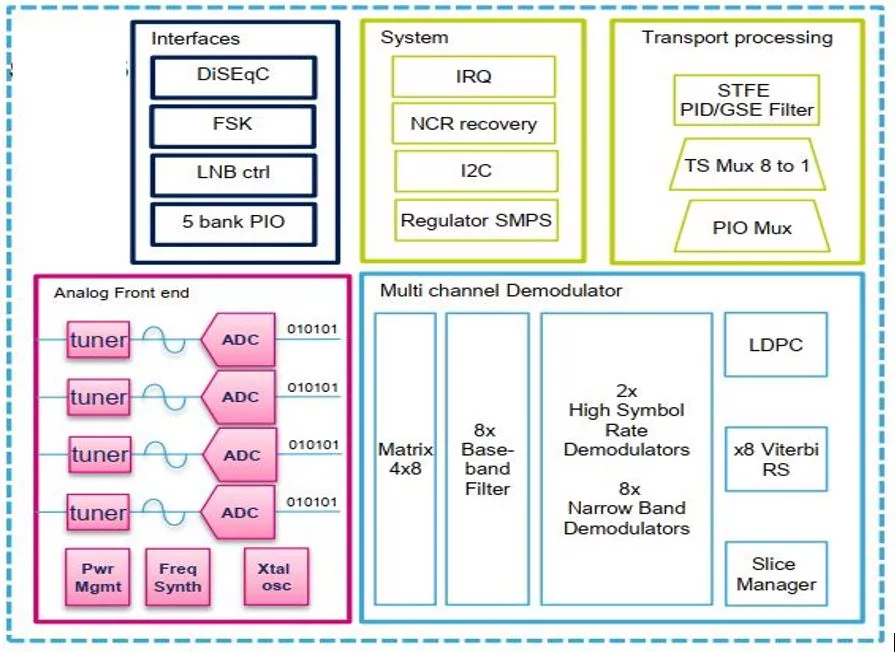
This is a high-performance, dual high-symbol-rate (HSR) DVB-S2/S2X demodulator IP extarcted from production chipsets with integrated tuner and silcon proven technology. The demodulators are compliant with Annex M of the DVB-S2 specification EN 302 307 and can demodulate signals up to 500 Msymbol/s. Each HSR demodulator may demodulate up to 2 slices. This implements 8 multi-standard demodulators capable of DVB-S, DTV legacy, DVB-S2 and DVB-S2X broadcast-profile signal processing.
This IP incorporates a high-speed DVB-S2 forward error corrector (FEC) which is designed to handle up to 720 Mchannel-b/s at its input. This allows for 8 simultaneous 8PSK decodes at 30 Msymbol/s. This capacity is shared between the demodulators and may be allocated at will, provided that the maximum capacity limit is not exceeded.This IP features four integrated full-band capture tuners which cover the band 950 to 2150 MHz. The signal is sampled by high-performance analog to digital converters with built in anti-aliasing filters.These ADCs connect to a high-speed digital multiplexer which allows any tuner input to feed any of the 8 demodulators.
This implements full S2 and S2X interactive services capability with short frames and full-ACM functionality including MODCOD blocking. An NCR PLL compatible with both MPEG2 and GSE streams has been implemented and may be associated with any of the demodulators to assure return-channel synchronization. A transport stream processor is able to filter on PIDs, carry out PCR re-stamping and conduct PID relabeling. In this way the wanted program streams can be, for example, output on a single multiplexed bus thus reducing wiring complexity and saving board space. The transport stream processor is also capable of handling GSE, GSE-lite, IP streams and can output raw, baseband fames.
This integrates all the features needed to provide a low-cost multi channel broadcast satellite receiver solution including: integrated crystal oscillator, SMPSs for single wire supply, DiSEqC controller, I2C repeater, FSK modem, ancillary DACs and ADCs and many unattributed general-purpose input-output ports for peripheral control. Advanced power-saving features have been implemented, the LDPC stops once the solution is sufficiently converged and the various blocks of the IC (tuner, demodulator, LDPC, Legacy FEC, and so on) may be completely shut down if not required. The device also supports Wake-on-network PID.
Provider
T2M GmbH is the leading Global Technology Company supplying state of the art complex semiconductor connectivity IPs and KGDs, enabling the creation of complex connected devices for Mobile, IoT and Wearable markets.
T2M's unique SoC White Box IPs are the design database of mass production RF connectivity chips supporting standards including Wifi, BT, BLE, Zigbee, NFC, LTE, GSM, GNS. They are available in source code as well as KGD for SIP / modules.
With offices in USA, Europe, China, Taiwan, South Korea, Japan, Singapore and India, T2M’s highly experienced team provides local support, accelerating product development and Time 2 Market.
Learn more about Modulation Demodulation IP core
This paper focuses on how direct RF sampling architecture has proved to be a felicitous approach for RF data conversion. The progress in converter technology has made it possible to increase the sampling rates and support very large bandwidth and multiple operating RF bands.
Synopsys is now shipping support for Bluetooth® 5.4, the latest specification from the Bluetooth SIG (Special Interest Group). The enhancements in Bluetooth 5.4 will open additional markets and use cases. This is one of the many inflection points in the Bluetooth Low Energy market that will be discussed in this paper.
Carriers are now deploying 5G across the globe driven by the need to keep up with relentless mobile data growth. 5G New Radio (NR) operates at higher frequencies to increase bandwidth, but at the expense of range. There will therefore be a need for a much larger number of 5G RUs to provide the same coverage. The availability of cost-effective, reliable and open 5G radio units is therefore critical.
This paper presents the design and performance of a key RF circuit necessary for the realization of a reconfigurable, integrated RF front-end: a tunable frequency, selectable bandwidth, on-chip, “SAW replacement” filter. The on-die tunable filter presented here has a tunable center frequency up to 1 GHz, a selectable bandwidth up to 40 MHz, and an adjacent channel rejection down to 60 dB.
To meet the demands for the multi-band, multi-mode wireless standards in the current market, a highly integrated wireless receiver (RX) is desired. CMOS technology has become the technology of choice for the integrated receiver design.
An efficient IP reuse strategy relies on IP blocks with wide applicability. That makes generic blocks, such as programmable processors preferable. However, in many applications such as handheld wireless terminals, additional silicon area and power consumption compared to fixed function solutions can not be accepted.