How Secure DDR Interfaces Protect DRAM from Memory Attacks
Brett Murdock, Dana Neustadter (Synopsys)
Today’s consumers generate and consume large volumes of data and video, exploding the need for data-intensive processing requirin…
Today’s consumers generate and consume large volumes of data and video, exploding the need for data-intensive processing requiring high memory bandwidth. The Cadence Denali DDR IP is a family of high-speed on-chip interfaces to external memories supporting these high-performance requirements with products that are optimized for each application’s needs
The latest, the DDR5/4 PHY IP for TSMC 7nm, is comprised of architectural improvements to its highly successful predecessor, achieving breakthrough performance, lower power consumption, and smaller overall area. The application optimized DDR PHY IP can achieve speeds up to 4800Mbps. Low-power features include the addition of VDD low-power idle state in the PHY, and power-efficient clocking during low-speed operation for longer battery life and greener operation. Redesigned I/O elements reduce overall area by up to 20%.
The PHY IP is developed by experienced teams with industry-leading domain expertise and extensively validated with multiple hardware platforms. It is engineered to quickly and easily integrate into SoCs, and is verified with the Cadence Denali Controller IP for DDR as part of a complete memory subsystem solution. The PHY IP is designed to connect seamlessly and work with a thirdparty DFI-compliant memory controller.
Product Details
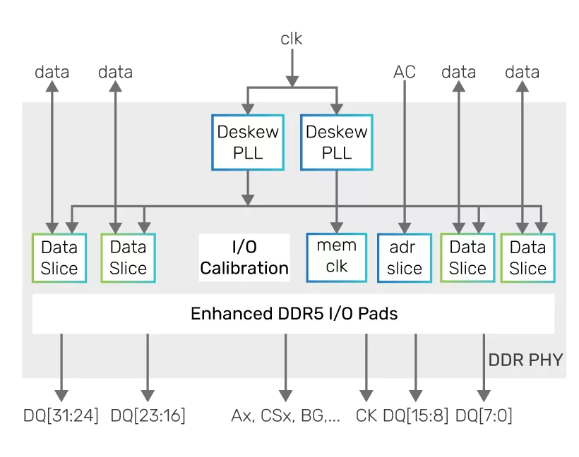
The DDR PHY IP consists of a DFI interface to the memory controller, external register interface (configuration and test), PHY control block (initialization and calibration logic), and configurable data slices.
The DDR PHY IP is a high-performance DQS-delay architecture that uses programmable clock delay lines to align write data, read data capture, and DQS gating from the I/O pads across the DFI interface to the memory controller.
PHY Architecture
To optimize the DDR interface implementation, the DDR PHY IP provides complete flexibility with process, library, floorplan, I/O pitch, packaging, metal stackup, routing, and other physical parameters.
The DDR PHY IP is implemented with a slice-based architecture that supports a wide range of memory classes and data rates.
Data Slice and Address/Control Slices
The data slice is an 8-bit-wide design that interfaces to the DQ, DM, and DQS connections of the DRAM. The data slice is duplicated to create the appropriate data width, allowing flexibility to adjust to meet the requirements of the systems or applications.
The address and address/control slices interface to the control, command, and address connections of the DRAM. The address and address/control slices are duplicated to create the appropriate widths for different protocols or combination of protocols, allowing flexibility to adjust the number of control, command, and address signals as needed.
External Register Interface
The external register interface is a Cadence-proprietary interface to access the data slice registers
PHY Control Block
The DDR PHY IP control block provides initialization and calibration logic for training the DQS alignment for each data slice.
| Foundry | Node | Process | Maturity |
|---|---|---|---|
| TSMC | 7nm | N7+ | Available on request |
Note: some files may require an NDA depending on provider policy.

DDR5/4 PHY for TSMC 7nm is a DDR IP core from Cadence Design Systems, Inc. listed on Semi IP Hub. It is listed with support for tsmc Available on request.
Engineers should review the overview, key features, supported foundries and nodes, maturity, deliverables, and provider information before shortlisting this DDR IP.
Yes. Buyers can compare this product with similar semiconductor IP cores or IP families based on category, provider, process options, and structured technical specifications.