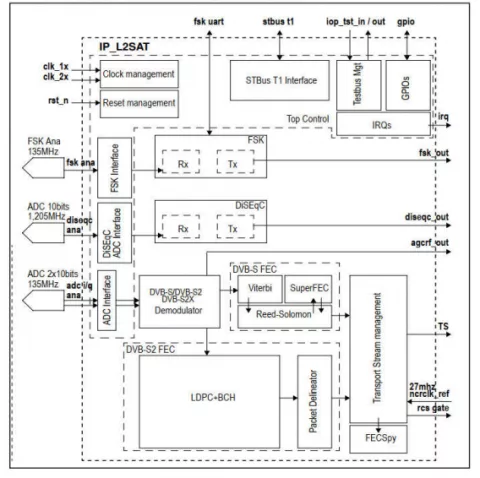
Overview
This is NarrowBand demodulator IP is silicon proven and extratced from production chipsets, it performs demodulation according to DVB-S, legacy DirectTV, DVB-S2 and DVB-S2X specifications. The input signal from the tuner is A-to-D converted on 10 bits. The DC offset, amplitude mismatch and quadrature error are corrected and the AGC signal level to the tuner is calculated. The carrier frequency offset is corrected. Then the signal is sub sampled and Nyquist root filtered. The signal amplitude is controlled through the second stage (AGC2) block. The pilots, when present, are used to help phase lock to the symbol stream. The signal is equalized, descrambled, and passed to the FEC. An internal state machine controls the automatic acquisition of a channel with various entry points, including warm start (known symbol frequency, small carrier offset), cold start (known symbol frequency and large carrier frequency offset), and blind search (all parameters unknown).
The DVB S2X NarrowBand IP main demodulation path takes its data from a dual ADC sampling the signals I/Q coming from an external tuner. The ADC is clocked at 135MHz and the data are on 10bits. After demodulation, the data is sent either to a DVB-S Forward Error Correction (FEC) path or a DVB-S2 FEC path.
The DVB-S FEC is based on a Viterbi and Reed-Solomon decoders. A SuperFEC mode is also implemented where a second Viterbi block is added to improve the performances. The DVB-S2 FEC is based on a LDPC+BCH decoder and a packet delineator block needed to extract the physical packets (MPEG or GSE) from the FEC frame. The decoded & corrected data is then sent to a transport stream interface managing standard TS-based transmission to the back-end decoder. In addition to this main demodulation path, peripheral interfaces are integrated, a DiSEqC and an FSK interfaces.They are both protocols to communicate with the LNB antenna on the coaxial cable.
Provider
T2M GmbH is the leading Global Technology Company supplying state of the art complex semiconductor connectivity IPs and KGDs, enabling the creation of complex connected devices for Mobile, IoT and Wearable markets.
T2M's unique SoC White Box IPs are the design database of mass production RF connectivity chips supporting standards including Wifi, BT, BLE, Zigbee, NFC, LTE, GSM, GNS. They are available in source code as well as KGD for SIP / modules.
With offices in USA, Europe, China, Taiwan, South Korea, Japan, Singapore and India, T2M’s highly experienced team provides local support, accelerating product development and Time 2 Market.
Learn more about Modulation Demodulation IP core
This paper focuses on how direct RF sampling architecture has proved to be a felicitous approach for RF data conversion. The progress in converter technology has made it possible to increase the sampling rates and support very large bandwidth and multiple operating RF bands.
Synopsys is now shipping support for Bluetooth® 5.4, the latest specification from the Bluetooth SIG (Special Interest Group). The enhancements in Bluetooth 5.4 will open additional markets and use cases. This is one of the many inflection points in the Bluetooth Low Energy market that will be discussed in this paper.
Carriers are now deploying 5G across the globe driven by the need to keep up with relentless mobile data growth. 5G New Radio (NR) operates at higher frequencies to increase bandwidth, but at the expense of range. There will therefore be a need for a much larger number of 5G RUs to provide the same coverage. The availability of cost-effective, reliable and open 5G radio units is therefore critical.
This paper presents the design and performance of a key RF circuit necessary for the realization of a reconfigurable, integrated RF front-end: a tunable frequency, selectable bandwidth, on-chip, “SAW replacement” filter. The on-die tunable filter presented here has a tunable center frequency up to 1 GHz, a selectable bandwidth up to 40 MHz, and an adjacent channel rejection down to 60 dB.
To meet the demands for the multi-band, multi-mode wireless standards in the current market, a highly integrated wireless receiver (RX) is desired. CMOS technology has become the technology of choice for the integrated receiver design.
An efficient IP reuse strategy relies on IP blocks with wide applicability. That makes generic blocks, such as programmable processors preferable. However, in many applications such as handheld wireless terminals, additional silicon area and power consumption compared to fixed function solutions can not be accepted.