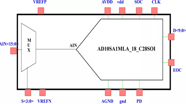
Overview
10-bit successive approximation Analog-to-Digital Converter (ADC) is designed for high-performance applications. Utilizing 28FDSOI technology with process options including 6 Metal (5+1), 8 Metal
(6+2), and 10 Metal (6+2+2), this ADC achieves exceptional performance while maintaining a compact silicon footprint.
With a parallel 10-bit output, this ADC offers a conversion time of 1 µs and a sampling frequency of 1 Msps, making it suitable for applications
requiring fast and accurate analog-to-digital conversion. In terms of performance, the ADC delivers exceptional accuracy with Integral Non-Linearity (INL) of less than ±1 LSB and Differential Non�Linearity (DNL)of less than ±0.5 LSB, ensuring precise conversion of analog signals into digital data.
Overall, this ADC offers high-performance analog�to-digital conversion in a compact and efficient
package, making it ideal for a wide range of
applications including industrial automation,
medical imaging, and telecommunications.
Provider
T2M GmbH is the leading Global Technology Company supplying state of the art complex semiconductor connectivity IPs and KGDs, enabling the creation of complex connected devices for Mobile, IoT and Wearable markets.
T2M's unique SoC White Box IPs are the design database of mass production RF connectivity chips supporting standards including Wifi, BT, BLE, Zigbee, NFC, LTE, GSM, GNS. They are available in source code as well as KGD for SIP / modules.
With offices in USA, Europe, China, Taiwan, South Korea, Japan, Singapore and India, T2M’s highly experienced team provides local support, accelerating product development and Time 2 Market.
Learn more about ADC IP core
This paper introduces a novel closed-loop testing methodology for efficient linearity testing of high-resolution Successive Approximation Register (SAR) Analog-to-Digital Converters (ADCs). Existing test strategies, including histogram-based approaches, sine wave testing, and model-driven reconstruction, often rely on dense data acquisition followed by offline post-processing, which increases overall test time and complexity.
Analog to digital converters have three key input ports along with data output ports as per digital resolution requirements. These inputs ports are Analog Signal, Reference and Clock. If we compare across most of the converter architectures then clock frequency is directly related to output data rate and latency of the data conversion.
The growing availability of digital ICs like microcontrollers, microprocessors, and field-programmable gate arrays (FPGAs) allows developers to use complex digital processing techniques rather than analog signal conditioning. For this reason, analog-to-digital converters (ADCs) have become a widely-used component in mixed-signal circuits.
In high end RF systems, such as 5G radios, the requirements are so stringent that the source of this strongest unwanted tone can be the PLL. This article outlines how spurs in the input clock to the ADC or DAC may limit the SFDR. This in turn will set the requirements for the spurs for the input clock (from a PLL), in order to achieve a specific SFDR.
Power-sensitive applications such as Internet-of-Things (IoT) require a comprehensive power savings strategy within the system-on-chip (SoC). Techniques relying solely on the use of traditional power down modes and low supply voltage may not be enough to achieve the required power targets. The analog block is often assumed to be too sensitive and not compatible with aggressive power management techniques.
When continuously running a high speed ADC, it can be a challenge to deal with the firehose of raw data available at the output. To use City Semiconductor’s 2.5 GS/s 12-bit ADC, for example, 30 gigabits per second of data have to be accepted.