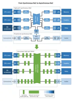
ANoC, a clock-less interconnect solution, aimed at simplifying the design of complex SoC, using standard synchronous tools & flow and achieving:
- Ultra-low-latency
- Ultra-Low-power consumption thanks to event driven communication
- Flexibility and robustness
Asynchronous Network on Chip IP
Overview
Key Features
- High performance interconnects, Ultra-low-latency and Deep pipelining
- Packet-based NoC transfers able to encapsulate recent communication protocols
- Quasi-delay-insensitive robust asynchronous design
- Ultra-low-power consumption thanks to event driven communication
- Generic NoC design (arbitrary number of connections, topology, data width, …), with flexible IP blocks:
- Routers, switches
- Flexible pipelining
- Globally-asynchronous locally synchronous domain crossing interfaces
- Size converters
- 3D Links
- Efficient low latency point to point links
- Used for long distance high throughput communication (in constrained SoC floorplan)
- Deep pipelining to tune the target throughput
- Compatible with traditional protocols such as AXI, Q-AXI, Q-AHB
- Easier implementation & SoC-level timing closure
- Design methodology:
- use standard synchronous tools & flow
- Silicon-proven
- 2D implementation on different technology nodes from 130nm down to 28nm
- 3D implementation with heterogeneous technologies (65nm/28 nm FDSOI) on the INTACT silicon prototype, a High-Performance Processor with 6 Chiplets of 16 cores each 3D stacked on an active interposer.
- Performance evaluation in 10nm FinFET
Benefits
- Performance gains of the ANoC compared to classical synchronous NoC:
- Power : Average gain up to 2-3x thanks to event-driven logic (minimal dynamic switching) and absence of clock tree power consumption
- Throughput : Internal bit-level datarate improvement up to 2x in typical usage, potentially allowing serialization of wide data words to narrower internal channels
- Latency:
- At NoC level (physical layer): gain up to 3x
- At system level (including network interfaces): gain up to 2x thanks to reduced router latency and reduced number of resynchronization cycles
- Area : Demonstrated area overhead of only 10% on the interconnect on a 64 bits-width data path thanks to 50% smaller clock domain-crossing interfaces
- Physical implementation
- Fast interconnect timing closure
- Full timing decoupling between core clock domains during place & route at top level
- Variability: Natural robustness to any source of Process, Voltage, Temperature (PVT) variations thanks to delay-insensitive design style
Block Diagram

Applications
- Solution dedicated for many-core and accelerator architectures for :
- Automotive and Transport
- Embedded systems and set-top boxes
- Health and Well being
- High-end Computing
Technical Specifications
Related IPs
- GPS/Galileo/GLONASS System on Chip based on "Leon 3" CPU
- MIPI C-PHY-D-PHY Combo PHY IP on TSMC 28nm HPC+
- High speed NoC (Network On-Chip) Interconnect IP
- UCIe/BoW BlueLynx™ Dual Mode PHY and subsystem IP for chiplet interconnect
- Universal Asynchronous Receiver / Transmitter
- Universal Asynchronous Receiver / Transmitter